(China (Mainland))

Product Summary
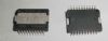
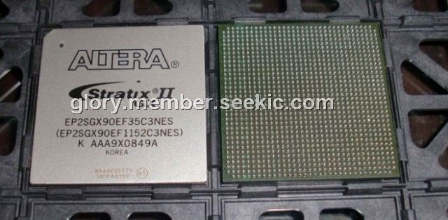
The EP2SGX90EF35C3NES is a member of Stratix II GX family which is Altera’s third generation of FPGAs to combine high-speed serial transceivers with a scalable, high-performance logic array. The EP2SGX90EF35C3NES includes 4 to 20 high-speed transceiver channels, each incorporating clock and data recovery unit (CRU) technology and embedded SERDES capability at data rates of up to 6.375 gigabits per second (Gbps). The transceivers are grouped into four-channel transceiver blocks and are designed for low power consumption and small die size. The Stratix II GX FPGA EP2SGX90EF35C3NES technology is built upon the Stratix II architecture and offers a 1.2-V logic array with unmatched performance, flexibility, and time-to-market capabilities. This scalable, high-performance architecture makes the EP2SGX90EF35C3NES ideal for high-speed backplane interface, chip-to-chip, and communications protocol-bridging applications.
Parametrics
EP2SGX90EF35C3NES absolute maximum ratings: (1)VCCINT, Supply voltage With respect to ground: –0.5 to 1.8 V; (2)VCCIO, Supply voltage With respect to ground: –0.5 to 4.6 V; (3)VCCPD, Supply voltage With respect to ground: –0.5 to 4.6 V; (4)VI DC, input voltage: –0.5 to 4.6 V; (5)IOUT, DC output current, per pin: –25 to 40 mA; (6)TSTG, Storage temperature No bias: –65 to 150℃; (7)TJ, Junction temperature BGA packages under bias: –55 to 125℃.
Features
EP2SGX90EF35C3NES features: (1)TriMatrix memory consisting of three RAM block sizes to implement true dual-port memory and first-in first-out (FIFO) buffers with performance up to 550 MHz; (2)Up to 16 global clock networks with up to 32 regional clock networks per device region; (3)High-speed DSP blocks provide dedicated implementation of multipliers (at up to 450 MHz), multiply-accumulate functions, and finite impulse response (FIR) filters; (4)Up to four enhanced PLLs per device provide spread spectrum, programmable bandwidth, clock switch-over, real-time PLL reconfiguration, and advanced multiplication and phase; (5)shifting; (6)Support for numerous single-ended and differential I/O standards; (7)High-speed source-synchronous differential I/O support on up to 71 channels; (8)Support for source-synchronous bus standards, including SPI-4 Phase 2 (POS-PHY Level 4), SFI-4.1, XSBI, UTOPIA IV, NPSI, and CSIX-L1; (9)Support for high-speed external memory, including quad data rate (QDR and QDRII) SRAM, double data rate (DDR and DDR2) SDRAM, and single data rate (SDR) SDRAM; (10)Support for multiple intellectual property megafunctions from Altera MegaCore functions and Altera Megafunction Partners Program (AMPPSM) megafunctions; (11)Support for design security using configuration bitstream encryption; (12)Support for remote configuration updates.
Diagrams
 |
 EP2S |
Other |
|
Data Sheet |
Negotiable |
|
||||||
 |
EP2S130F1020C3 |
|
IC STRATIX II FPGA 130K 1020FBGA |
Data Sheet |
|
|
||||||
|
EP2S130F1020C3N |
|
IC STRATIX II FPGA 130K 1020FBGA |
Data Sheet |
|
|
||||||
|
EP2S130F1020C4 |
|
IC STRATIX II FPGA 130K 1020FBGA |
Data Sheet |
|
|
||||||
|
EP2S130F1020C4N |
|
IC STRATIX II FPGA 130K 1020FBGA |
Data Sheet |
|
|
||||||
|
EP2S130F1020C5 |
|
IC STRATIX II FPGA 130K 1020-FBG |
Data Sheet |
|
|
||||||