(China (Mainland))

Product Summary
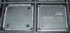
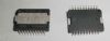
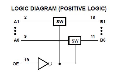
The SN74CB3T3245PWR is a high-speed TTL-compatible FET bus switch with low ON-state resistance (ron), allowing for minimal propagation delay. The device fully supports mixed-mode signal operation on all data I/O ports by providing voltage translation that tracks VCC. The SN74CB3T3245PWR supports systems using 5-V TTL, 3.3-V LVTTL, and 2.5-V CMOS switching standards, as well as user-defined switching levels. The SN74CB3T3245PWR is an 8-bit bus switch with a single ouput-enable (OE) input and a standard 245 pinout. When OE is low, the 8-bit bus switch is ON, and the A port is connected to the B port, allowing bidirectional data flow between ports. When OE is high, the 8-bit bus switch is OFF, and a high-impedance state exists between the A and B ports. This SN74CB3T3245PWR is fully specified for partial-power-down applications using Ioff. The Ioff feature ensures that damaging current will not backflow through the device when it is powered down. The SN74CB3T3245PWR has isolation during power off.
Parametrics
SN74CB3T3245PWR absolute maximum ratings: (1)VCC, Supply voltage range: –0.5 to 7 V; (2)VIN, Control input voltage range: –0.5 to 7 V; (3)VI/O, Switch I/O voltage range: –0.5 to 7 V; (4)IIK, Control input clamp current VIN < 0: –50 mA max; (5)II/OK, I/O port clamp current VI/O < 0: –50 mA max; (6)II/O: ON-state switch current: ±128 mA max; Continuous current through VCC or GND: ±100 mA max; (7)θJA, Package thermal impedance: DBQ package: 68℃/W; DGV package: 92℃/W; DW package: 58℃/W; PW package: 83℃/W; (8)Tstg, Storage temperature range: –65 to 150 ℃.
Features
SN74CB3T3245PWR features: (1)Standard 245-Type Pinout; (2)VCC Operating Range From 2.3 V to 3.6 V ; (3)Data I/Os Support 0- to 5-V Signaling Levels(0.8 V, 1.2 V, 1.5 V, 1.8 V, 2.5 V, 3.3 V, 5 V); (4)Output Voltage Translation Tracks VCC ; (5)Supports Mixed-Mode Signal Operation on All Data I/O Ports: 5-V Input Down to 3.3-V Output Level Shift With 3.3-V VCC; 5-V/3.3-V Input Down to 2.5-V Output Level shift With 2.5-V VCC ; (6)Control Inputs Can Be Driven by TTL or 5-V/3.3-V CMOS Outputs; (7)Ioff Supports Partial-Power-Down Mode Operation; (8)Latch-Up Performance Exceeds 250 mA Per JESD 17; (9)5-V-Tolerant I/Os With Device Powered Up or Powered Down; (10)ESD Performance Tested Per JESD 22: 2000-V Human-Body Model (A114-B, Class II); 1000-V Charged-Device Model (C101); (11)Bidirectional Data Flow With Near-Zero Propagation Delay ; (12)Low ON-State Resistance (ron) Characteristics (ron = 5 Ω Typ); (13)Supports Digital Applications: Level Translation, PCI Interface, USB Interface, memory Interleaving, Bus Isolation; (14)Low Input/Output Capacitance Minimizes Loading (Cio(OFF) = 5 pF Typ) ; (15)Ideal for Low-Power Portable Equipment; (16)Data and Control Inputs Provide Undershoot Clamp Diodes; (17)Low Power Consumption (ICC = 40 uA Max).
Diagrams
| Image | Part No | Mfg | Description |  |
Pricing (USD) |
Quantity | ||||||||||||
|---|---|---|---|---|---|---|---|---|---|---|---|---|---|---|---|---|---|---|
 |
 SN74CB3T3245PWR |
Texas Instruments |
Digital Bus Switch ICs 8-Bit FET 2.5/3.3V Lo-Vltg Bus Switch |
Data Sheet |
|
|
||||||||||||
|
SN74CB3T3245PWRE4 |
Texas Instruments |
Digital Bus Switch ICs 3.3-V ABT Octal Bus Trncvr W/3-St Otpt |
Data Sheet |
|
|
||||||||||||
|
SN74CB3T3245PWRG4 |
Texas Instruments |
Digital Bus Switch ICs 8B FET 2.5V 3.3V LO VLTG Bus Switch |
Data Sheet |
|
|
||||||||||||